World of CPU GPU & FPGA, Simplified!
World of CPU GPU & FPGA, Simplified!
Since the invention of abacus, the evolution of calculations to computing is aligned to the human inventions since they used abacus for the operation of addition and subtraction; however, this primitive device underwent extensive transformation the time has witnessed. We have seen the most relevant cousin of abacus transforming into calculators as special purpose devices but the transformation paradigm of making most complex calculations kept the ball rolling when Blaise Pascal (1623–1666) invented the first practical mechanical machine that had a series of interlocking cogs / gears that could add and subtract decimal numbers.
In 1971, Intel launched first microprocessor Intel 4004 that had 2300 transistors with pMOS technology, which could process 46 number of instructions with a 740KHz clock speed used in and it was used in the Busicom 141-PF calculator. In subsequent year 1972, Intel launched 8008 used in personal computers, Micral and SCELBI, that could process 48 instructions with 3400 transistors.
The journey did not stop then and continues to surprise us with modern family of processors that forked out greater possibilities for general purpose processors to niche embedded integrated circuits within the devices such as cameras, mobile phones, washing machines and yes our Cloud Computing too, this changed our world onto a digital era we experience and count on each day touching everyone’s life! The latest processors have multiple cores, with clock speeds counted in GHz, turbo speeds, L2 and L3 Cache to take the computing to next level… Just to put the facts on the table, A dual core Skylake Intel SoC contains 1.75 Billion transistors so the I/O controllers, GPU and SRAM caches account for 1.316 Billion transistors (1.75B minus 2x 217M for cores). With that in mind an i9-9900K would have around 3.052 Billion transistors, imagine this was released last year, i.e 2018..
The traction of modern GPUs started in 1995 with the introduction of the first 3D graphic add-in cards, till then options for the industry were limited to 2D and non-PC architecture, and graphics cards were expensive, the game changer of GPU launched by NVIDIA called GeForce 256, was a single-chip processor with integrated transform, lighting, triangle setup/clipping, and rendering engines that is capable of processing a minimum of 10 million polygons per second, the gaming fraternity was Indeed overjoyed! By now you must have identified that there is a different clan of processors called GPU which distinguished itself from the world that only knew on CPU for general purpose usage.
So, What’s the difference between CPU and GPU?
A central processing unit (CPU), also called a central processor or main processor, is the electronic circuitry within a computer that executes instructions that make up a computer program. CPU comprises the arithmetic logic unit (ALU) accustomed quickly to store the information and perform calculations and Control Unit (CU) for performing instruction sequencing as well as branching. CPU interacts with more computer components such as memory, input and output for performing instruction. Inside the CPU the instructions are sequenced and processed serially, that means it can perform operations in sequence, whereas in GPU leverages parallel processing wherein multiple ALUs process large amount of instructions in parallel. CPUs race through a series of tasks requiring lots of interactivity. Calling up information from a hard drive in response to user’s keystrokes, for example.
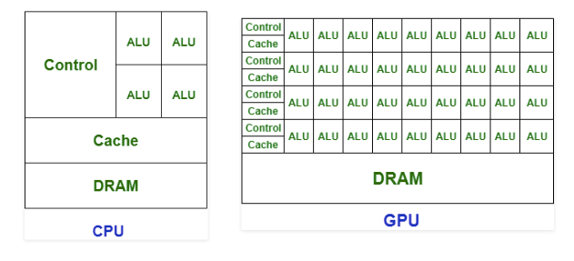
On the other hand, GPUs break complex instructions into thousands or millions of separate tasks and work on them out at once. Thus it is ideal for graphics, where textures, lighting and the rendering of shapes have to be done at once to keep images flying across the screen or processing thousands of tiny tasks such as ingesting data from millions of IoT devices or run repetitive arithmetic operations of millions of records of columnar databases etc.
Architecturally, the CPU is composed of just a few cores with lots of cache memory that can handle a few software threads at a time. In contrast, a GPU is composed of hundreds of cores that can handle thousands of threads simultaneously. GPUs perform much more work for every unit of energy than CPUs. Like NVIDIAs CUDA enables developers to speed up compute-intensive applications by harnessing the power of GPUs for the parallelizable part of the computation.
Taking the parallel processing to next level with FPGA?
Now, instead of the common approach of writing some software for an instruction-based architecture, such as a CPU or GPU, another approach is to design a special processor for this specific computation. Parallel processing is a method of simultaneously breaking up and running program tasks on multiple microprocessors, thereby reducing processing time. Ability to run the tasks on millions of Gate Arrays is what FPGA does. Simply put, FPGA is Field Programmable Gate Array (FPGA), a reconfigurable integrated circuit that is so agile that one can configure the FPGA to become any circuit you want to in real time yet dynamically. FPGA is made up of thousands of Configurable Logic Blocks (CLBs) embedded in an ocean of programmable interconnects. The CLBs are primarily made of Look-Up Tables (LUTs), Multiplexers and Flip-Flops. They can implement complex logic functions.
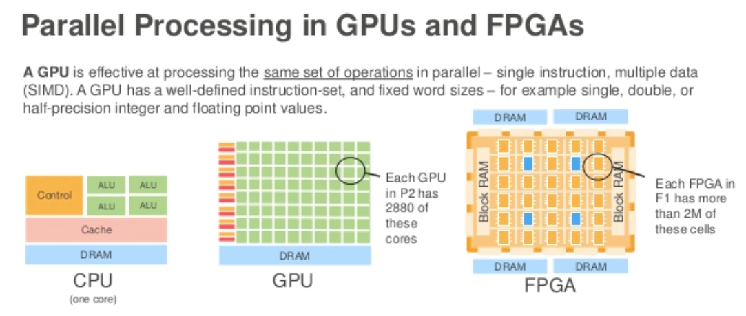
This is quite a bit different than the instruction-based hardware most programmers are used to, such as CPUs and GPUs since FPGA can be used to solve any problem which is computable. This is trivially proven by the fact that FPGAs can be used to implement a soft microprocessor, such as the Xilinx MicroBlaze or Altera Nios II. Just recently, Intel bought Altera, one of the largest producers of FPGAs to ensure they have significant presence in this segment too..
One of the advantage of FPGA lies in that they are significantly faster for some applications because of their parallel nature and optimality in terms of the number of gates used for certain processes. The connectivity in FPGA is direct to either network interface or sensor unlike for GPU or where you have to connect your source via the standardized buses (such as USB or PCIe) and depend on the operating system to deliver the data to your application.
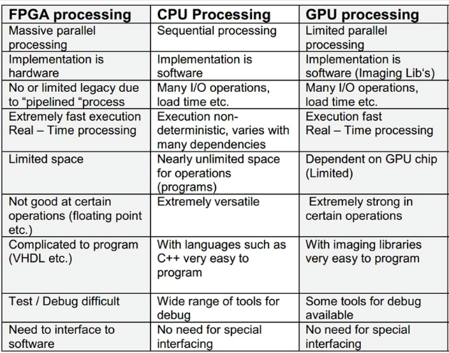
FPGAs are really much harder to program/configure than traditional instruction-based architectures used by CPUs and GPUs. High Level Synthesis (HLS) is now being used programming FPGAs using regular programming languages such as OpenCL or C++, allowing for a much higher level of abstraction yet has a higher learning curve and still an order of magnitude more difficult than programming instruction based systems, this results in lower adoption in the wider context of applications limiting its usage to higher and niche problem solving areas such as astrophysics, bioinformatics, device controllers, software-defined radio, random logic, ASIC prototyping, medical imaging, computer hardware emulation etc.
Modern Hybrids, the FPGA Accelerators
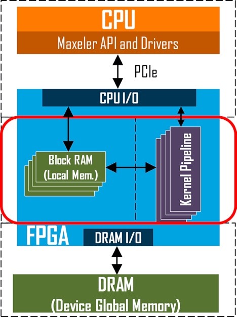
Since FPGAs value proposition sits between CPU and GPUs, many innovations on hybrid use of CPU and FPGAs as accelerators were invented and have seen good adoption, CPU offloads the complex tasks to FPGA connected via PCI express bus and combination accelerates the output thus using hybrid model both technologies are leveraged as value addition. This is a major shift in the approach when FPGA’s were paired with CPU’s to facilitate compute intensive operations. FPGA’s cannot adapt to new tasks as quickly as a general-purpose CPU, but they excel at repetitive operations that involve high throughput whereas CPU now orchestrates the instruction sequence keeping FPGA in the background running parallel processing of tasks.
The prominent Usecase of Artificial Intelligence...
Many of us would remember in early 90’s, computers have frequently complemented the CPU with special purpose accelerators for specialized tasks, known as coprocessors. Notable application-specific hardware units include video cards for graphics, sound cards, graphics processing units and digital signal processors. We can say this was the trigger to produce workload centric integrated chips / processors leading to GPUs, FPGAs and ASIC, Application Specific Integrated circuits). The difference in case of ASIC is that the resultant circuit is permanently drawn into silicon whereas in FPGAs the circuit is made by connecting a number of configurable blocks dynamically inline and called soft microprocessor.
As deep learning and artificial intelligence workloads rose in prominence in the 2010s, specialized hardware units were developed or adapted from existing products to accelerate these tasks eventually leading to a term “AI Accelerators” a class of microprocessor designed as hardware acceleration for running artificial neural networks, machine vision and machine learning workloads. As of 2016, GPUs were popular for AI work, and they continued to evolve in a direction to facilitate deep learning, both for training and inference in devices such as self-driving cars. GPU developers such as Nvidia NVLink are developing additional connective capability for the kind of dataflow workloads AI benefits from and have seen major traction on their efforts in the developer community.
The reprogrammable nature of an FPGA ensures the flexibility required by the constantly evolving structure of artificial neural networks. FPGAs also provide the custom parallelism and high-bandwidth memory required for real-time inferencing of a model. An FPGA can handle multiple workloads while keeping application performance at a high level and can adapt to changing workloads by switching among several programs.
The ability to be reprogrammed for multiple purposes is one of the main benefits of FPGA technology. Regarding AI-related solutions, separate blocks or an entire circuit can be reprogrammed to fit the requirements of a particular data processing algorithm. Some FPGA manufacturers are already working on implementing cloud-based FPGAs for AI workload acceleration and all kinds of applications requiring intense computing. Yet, the flexibility of FPGAs comes at the price of the difficulty of reprogramming the circuit. There aren’t enough skills available to cope up with the demand and even though using FPGAs for accelerating deep learning looks promising, only a few have tried to implement it in real life. For most AI solution developers, a more common tandem of GPUs and CPUs and combination of accelerators might look less problematic and easier due to their large-scale adoption and market penetration in the current eco system.
In Summary, As we read this article about CPU, GPU & FPGAs, there is a lot of research and active work happening to think of ways to accelerate processing / computing for different workloads. Google has Tensorflow Processing Units (TPUs), which promises an acceleration over and above current GPUs. Similarly Intel has added “Deep Learning Boost” (DLB) capabilities framework called Neon, alongside their leading CPUs and is working on creating faster FPGAs, which may provide higher flexibility and acceleration in coming days. In addition, the offerings from Cloud service providers is also increasing. We will see each of them emerge in coming months such as Digital Signal Processors (DSP) is yet another evolving option for processing data in real time. There are more than dozen key inventors having vision, plans and products in line with specialized chipsets that are focused to solve niche problems and provide frameworks around, Augmented / Virtual Reality (ARVR) AI/ML, Robotics, Biotechnology and Automation space and are making the difference too. The show continues to go on, what say?
***
Oct 2019. Compilation from various publicly available internet sources, authors views are personal.